
Why Large-Area Inspection Has Become a Measurement Problem
As packages outgrow the wafer, the constraint shifts from what a camera can see to what it can be trusted to measure.
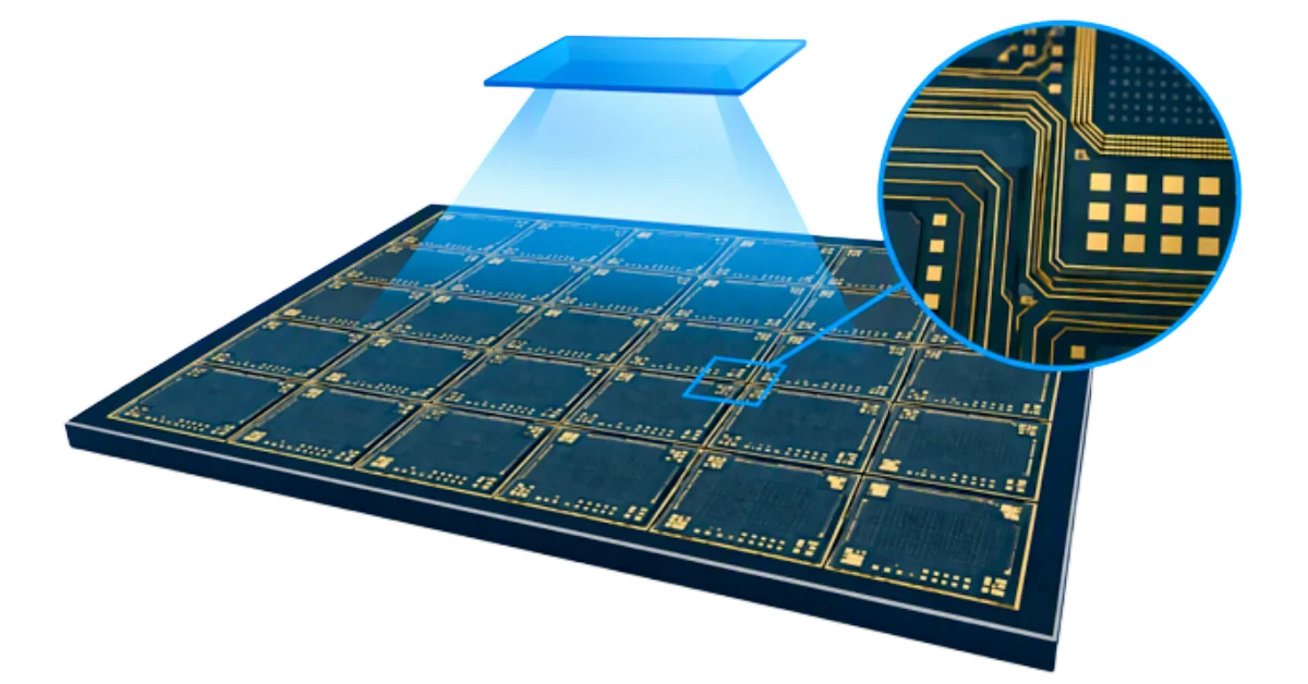
Most of the attention paid to semiconductor manufacturing follows the same direction: smaller nodes, finer features, tighter tolerances. Advanced packaging is pulling in the opposite direction at the same time. Packages are getting physically larger, and the features inside them are getting smaller. Inspection must accommodate both trends at once, and conventional approaches of building a large field of view are starting to strain under the combined demands.
Two trends running in opposite directions
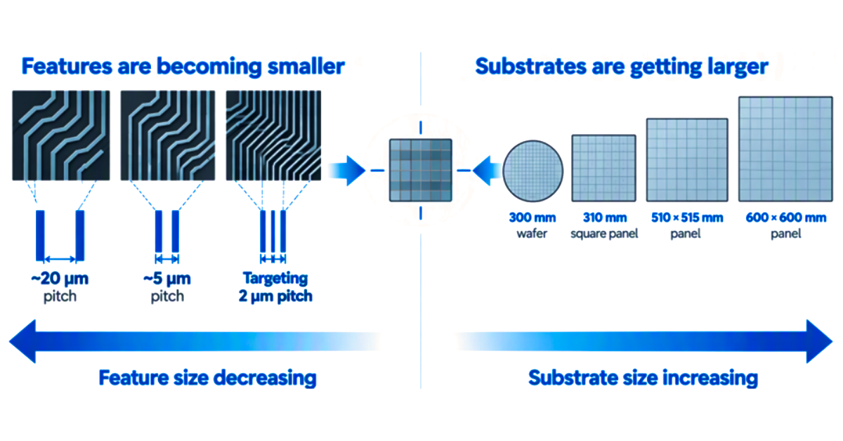
Fig 1. Advanced packaging is driving inspection requirements in two directions at the same time.
To support high-density fan-out, redistribution layer counts are moving from three layers to nine, while trace and bump pitches compress from roughly 20 microns to 5 microns. Manufacturers are targeting 2-micron pitches within the next five years, and process development work demonstrating a stable 2 µm line/space window has already been published.
Substrate formats are moving the other way, and the industry has not converged on a single answer. SEMI has standardized panel handling for 510 × 515 mm and 600 × 600 mm formats, while a separate SEMI task force was formed to develop carrier standards for 310 mm square panels, specifically to allow panel-level packaging to reuse existing 300 mm wafer infrastructure such as load ports and automated material handling. Two competing directions being standardized in parallel indicate that the industry has not yet determined which format will dominate.
An inspection system that once covered a 300 mm wafer at a given resolution is now being asked to cover several times that area, at several times the sensitivity, and maintain throughput. Those requirements do not scale together.
Why a larger field of view is not simply more pixels
Coverage and magnification trade against each other. Widening the field of view over a fixed sensor reduces the sampling of each feature; recovering that detail means either more pixels, more sensors, or more passes. Each of those has a cost, and the cost is not always where it is expected.
The conventional answer has been to build the field of view from several cameras and optical assemblies and then reconcile them in software. That approach works, and it has carried the industry a long way. However, it also brings a standing set of obligations with it:
- • Camera-to-camera calibration that must be maintained over temperature and time
- • Stitching and image reconstruction across boundaries
- • Alignment correction between imaging zones
- • Periodic recalibration as a maintenance task rather than a one-time step
None of these is difficult in isolation. Together, they mean that a portion of the system's accuracy is being maintained by procedure rather than guaranteed by design.
A seam is not a cosmetic problem. It is a false defect.
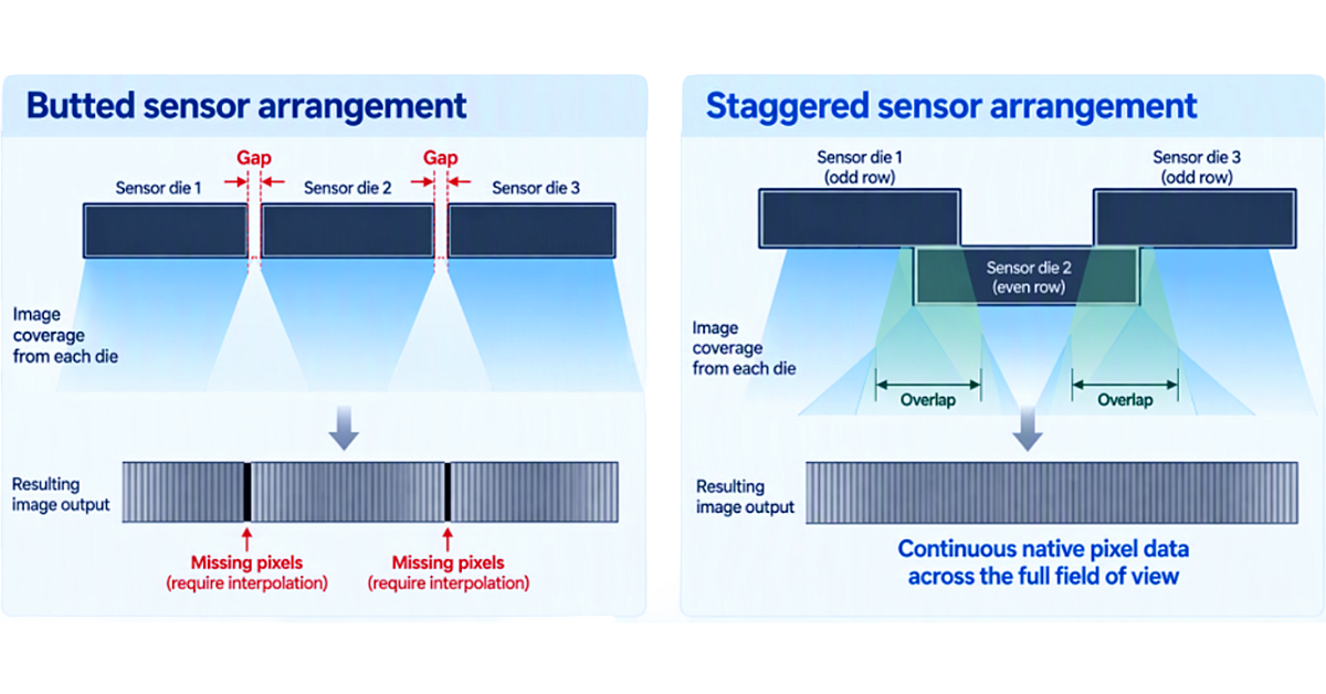
Fig 2. Sensor arrangement and image alignment determine whether native measurement data is maintained across the full inspection width.
The practical consequence of a boundary between sensors is not that the image looks worse. It is that the boundary can be classified as a defect, while a real defect sitting near it can be missed. The same effect is already documented at focus boundaries in packaging inspection, where surface height variation exceeds the depth of field of the optics and produces false defects on one side while hiding real ones on the other.
False defects are not neutral events. They quietly erode yield, inflate test cost, and mask the true health of the process because a false failure looks identical to a real one. Advanced packaging substrates make this worse in a specific way: heterogeneous surfaces of copper, dielectric and exposed silicon break the contrast assumptions that inspection recipes are built on, and nuisance rates rise accordingly.
The economics of a large panel then amplify every one of those calls. The arithmetic is unforgiving. A 510 × 515 mm panel populated with 120 × 120 mm packages yields sixteen units, so condemning one costs over six percent of the panel. Move to 150 × 150 mm packages and the same panel yields nine, putting a single false call above eleven percent. Where a fan-out panel might carry thousands of small packages and absorb an incorrect call almost invisibly, large-format substrates offer no such cushion. The larger the package, the more expensive it becomes to be wrong about it.
Warpage turns an imaging question into an optical one
The second pressure is mechanical, and the industry's understanding of it is changing. Warpage is no longer treated as a single global bow specification. Instead, it is increasingly understood as a collection of local shape signatures, including substrate bow, die tilt, redistribution layer variation, bonding and CMP effects, thermal mismatch. Each contributes at a different length scale and affects bonding, alignment and lithography differently.
Panel-level processing amplifies all of it. Larger geometries accumulate more stress across more heterogeneous materials, and processes that behave predictably on a 300 mm wafer do not automatically scale to a large rectangular panel. Optical measurement systems now must account for that deformation as a standing condition rather than an exception.
For a conventional lens, height variation changes magnification. A feature imaged closer to the lens measures larger than the identical feature at the nominal plane. On a flat 300 mm wafer that error may sit inside the tolerance. Across a warped panel, with several microns of local height variation, it does not.
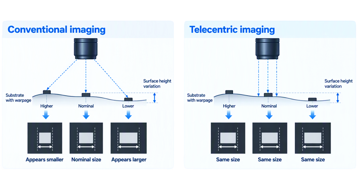
Fig 3. Telecentric imaging helps maintain a consistent image scale as object height varies, supporting more reliable inspection and measurement across large, warped substrates.
Telecentric optics remove that dependency: magnification stays constant regardless of surface height, so a measurement taken at the edge of a warped panel carries the same scale as one taken at the centre. This is the point at which large-area inspection shifts from being primarily a camera specification to being an optical architecture decision. Measurement stability is being determined before any software touches the image.
Inspection and metrology are converging on the same platform
Historically, these were separate activities with separate equipment. Detection asked whether something was wrong; measurement asked by how much. Advanced packaging has collapsed the distinction. Micro-bump coplanarity, RDL linewidth, die placement accuracy and warpage are all quantities, not observations, and they are increasingly expected from the same pass that performs defect detection.
That expectation changes what an inspection system is being asked to guarantee. It is no longer enough to see the entire substrate. The system has to produce numbers from any point on that substrate that are comparable to numbers from any other point, on any other tool, six months later.
The question equipment designers are left with
The industry has not settled on an answer. Panel formats have not yet converged on a common standard, and inspection approaches such as area-scan macro, line-scan, and hybrid architecture are all still in play.
What does appear settled is the shape of the requirement. Large-area inspection is becoming a measurement discipline. The properties that determine whether measurements can be trusted, such as continuity of coverage, stability under height variation, consistency across tools over time, are decided by the imaging architecture. They cannot simply be recovered later through software.
For equipment designers, that reframes the evaluation. The question is no longer simply which camera can resolve the smallest feature. It is which architecture can produce a consistent answer every time.