
Infrared Detector Sensor Materials
Introduction
Teledyne Judson Technologies is a global leader in the design and manufacture of high-performance infrared (IR) detectors, covering the spectrum from visible to very long wavelength infrared. To offer solutions that can detect across such a wide spectrum, we make use of a wide range of different sensor materials. This article will cover these materials, their characteristics, best applications, and more.
The featured sensor materials are as follows:
- InGaAs (Indium Gallium Arsenide)
- InAs (Indium Arsenide)
- InSb (Indium Antimonide)
- MCT (Mercury Cadmium Telluride, HgCdTe)
- T2SL (Type-II Superlattice)
Infrared detection performance is fundamentally defined by the semiconductor material used to make the sensor. Spectral response, detectivity (D*), imaging speed, operating temperature, stability, system complexity and many more are all material dependent.
To see the full range of Teledyne Judson Technology products, please refer to our Infrared Detector Selector Tool or Infrared Detector webpage.
Elemental Choices
No single semiconductor material optimally covers the entire IR range from near infrared (NIR) to far infrared (FIR), each semiconductor material has a characteristic bandgap and responsivity window. IR detectors are typically composed of multiple semiconductors and occupy specific IR regions, making it important to select the materials that can image most effectively in the regions you wish to capture.
The most widely used semiconductors for IR detectors are indium (In), gallium (Ga), arsenic (As), antimony (Sb), mercury (Hg), cadmium (Cd) and tellurium (Te), as outlined in Fig.1.
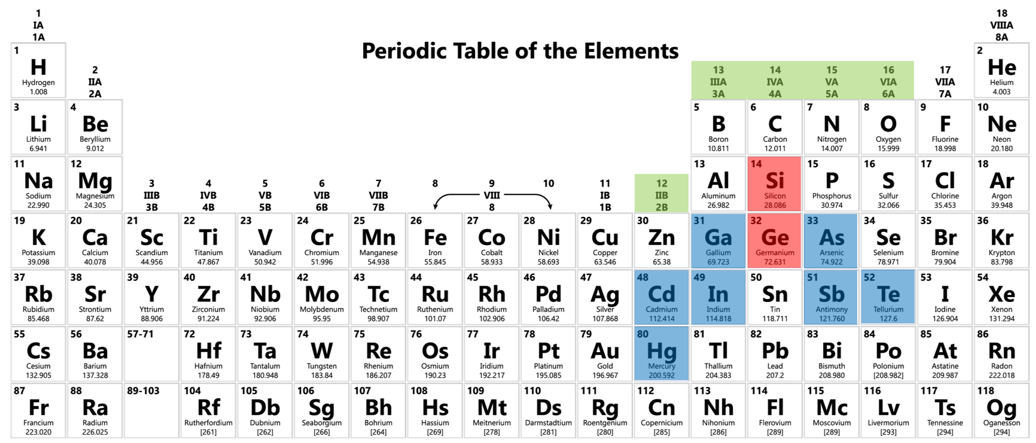
Figure 1: The current periodic table of elements, with suitable semiconductor elements for IR detectors highlighted in blue. Two other semiconductor elements are highlighted in red, namely silicon (Si, excellent visible light detector, but poor IR detector as it can only detect a max wavelength of ~1.1 µm) and germanium (Ge, can detect IR but is harder to tune, often results in sensors with higher noise, and has poor temperature stability). As these materials are also often referred to by the roman numerals of their group header (III-V or II-VI), these have also been highlighted in green.
Of the elements highlighted in Fig.1, all of them are semiconductors; they can detect light when photons with enough energy can move one of their electrons across the bandgap. As IR photons have lower energy than UV or visible photons, IR-detecting semiconductors typically have small bandgaps. These elements are also tunable, allowing certain combinations of elements to better detect certain regions of the IR spectrum.
As a result, most IR sensors are composed of a combination of two or more of these elements, each combination resulting in different performance, most significantly affecting IR detection wavelengths. The IR spectrum is wide, as seen in Fig.2, so we offer a correspondingly wide portfolio of detectors, as different applications demand fundamentally different detector characteristics, and a single-material approach would inevitably compromise performance in many of them.
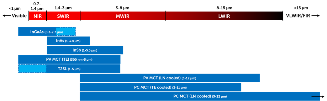
Figure 2: The IR spectrum and the detection ranges of each sensor material. The range includes near IR (NIR), short wave IR (SWIR), mid wave IR (MWIR), long-wave IR (LWIR) and beyond (very LWIR and far IR).
Each of these sensor materials can detect a different IR wavelength range, and each has a specific cutoff wavelength, where the sensitivity drops to 50% or less when compared to the peak value. Important to note is that the level of cooling can affect the cutoff, which is why Teledyne Judson Technologies offers uncooled, thermoelectric (TE) cooled and liquid nitrogen (LN) cooled devices, which all have different wavelength ranges, as seen in Fig.2.
This article explains the physics and practical performance of each material, describes the applications each serves best, and addresses two key comparative questions that arise frequently in detector selection: why choose InGaAs over germanium (Ge) for NIR/SWIR applications, and why choose cooled MCT over uncooled microbolometer technology for MWIR and LWIR sensing.
With this in mind, let’s look at the main sensor materials, product examples, and best applications.
InGaAs
Key Features
- NIR/SWIR detection
- Multiple cutoff wavelengths available, from 1.7 µm to 2.6 µm (as shown in Fig.3)
- Stable response vs. temperature
- Wide dynamic range
- High linearity
- No bias or cooling required
- Can be ordered integrated with an amplifier and TE controller for easy integration
Performance
InGaAs is a III-V compound semiconductor formed by alloying indium arsenide (InAs) and gallium arsenide (GaAs). The fraction of indium and gallium determines the material's bandgap and its cut-off. The most widely used composition (grown on an indium phosphide (InP) substrate) contains approximately 53% indium, giving a cut-off at around 1.7 µm. Extended-wavelength InGaAs is then produced by increasing the indium content and pushes the cut-off out to 1.9, 2.2, 2.4, or 2.6 µm, but this comes at the cost of increased dark current and more demanding growth requirements.
The standard InGaAs composition enables efficient photodetection without the need for cryogenic cooling, delivering excellent performance when uncooled or TE cooled, eliminating the bulk, power, cost, and complexity of a cryogenic cooling system. This also results in low dark currents and an overall low noise floor.
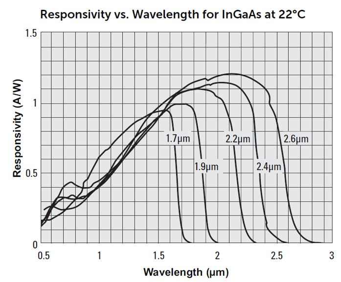
Figure 3: Responsivity vs wavelength for InGaAs sensors at 22 °C, highlighting five different cutoff options.
Key Applications
InGaAs is the dominant detector technology for the SWIR band and serves a broad range of established and growing application fields:
- SWIR imaging: industrial sorting, semiconductor inspection, solar cell characterization, document authentication, surveillance through haze
- Near-infrared spectroscopy: food and agricultural quality control, pharmaceutical in-line process monitoring
- Raman spectroscopy: optimal wavelength for Raman being ~785nm in the NIR
- Astronomy and remote sensing: extended InGaAs covers the J, H, and lower K atmospheric transmission windows.
- Medical and clinical diagnostics: pulse oximetry, tissue imaging, vein-finding.
- Gas detection: for CH4, CO, CO2, HCl, and other species with absorption features in the 1.5-2.5 µm window
- Telecommunications: fibre optics and test equipment (1.31 µm and 1.55 µm windows).
- Laser range-finding: LIDAR, and time-of-flight sensing at 1.0-1.55 µm.
InGaAs sensors can offer enhanced sensitivity, superior quantum efficiency, and minimal dark current providing researchers and engineers with advanced capabilities to tackle photonic challenges.
Why Use InGaAs Instead of Germanium?
Germanium (Ge) was historically the first semiconductor material widely used for NIR/SWIR detection, and it remains in use today in cost-sensitive applications. However, for the demanding requirements of modern SWIR sensing, spectroscopy, imaging, and communications, InGaAs offers a decisive combination of performance advantages that make it the preferred choice in the vast majority of applications, as outlined in the table below.
In general, InGaAs detectors have much lower dark currents (therefore cooling is optional), wider detection ranges, faster response times, can be grown as larger arrays, and have longer performance lifetimes when compared to Ge detectors.
| InGaAs | Germanium | |
| Spectral Range | 0.9-1.7 µm; up to 2.7 µm (extended) | 0.8-1.8 µm |
| Operating Temperature | Room temperature (TE-cooled optional) | Room temperature (TE-cooled for best performance) |
| Dark Current | Very low | Higher, rises steeply with temperature |
| Noise / NEP | Excellent, low noise floor | Higher shot noise at room temperature |
| Linearity / Dynamic Range | Excellent | Good but temperature sensitive |
| Cut-off Tunability | Tunable 1.7-2.6 µm (extended) | Fixed ~1.8 µm |
| Pixel / Array Maturity | Mature FPA and linear arrays available | Limited array availability |
| Relative Cost | Moderate | Lower |
| Best Use Case | Low-light SWIR, spectroscopy, 1.55 µm laser detection, >2 µm sensing | Cost-sensitive broadband NIR detection |
For modern SWIR detection, InGaAs has largely replaced Ge in high-performance applications.
Key Products
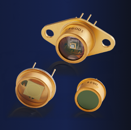
Teledyne Judson Technologies’ J22 and J23 series are high-performance, room temperature InGaAs detectors that operate over a spectral range from 1.7 µm to 2.6 µm. These detectors provide fast rise time, uniform response, excellent sensitivity, and long-term reliability for a wide range of applications.
InAs (Indium Arsenide)
Key Features
- MWIR detection, typical spectral range 1.0-3.8 µm
- Peak response in 2.0-3.5 µm region
- Operates at TE-cooled temperatures, uncooled not suitable
- Fast photoresponse
- Well-established material and growth processes
- Some InAs devices are photovoltaic and can be operated at zero volts
Performance
Indium arsenide (InAs) is a narrow-bandgap III-V semiconductor, the temperature-dependent bandgap places the spectral response window for InAs between ~1.0 µm and 3.8 µm, bridging the SWIR and MWIR bands. InAs is in a uniquely useful spectral position: it captures the high-reflectance SWIR region, the important 3-5 µm atmospheric transmission window where many gases absorb strongly, and the characteristic emission bands of high-temperature combustion.
Unlike InGaAs, InAs is not well-suited to room-temperature operation for most detector applications, as its narrow bandgap results in high thermally generated carrier concentrations at ambient temperatures, raising dark current to levels that degrade sensitivity. Cooling to temperatures in the range of 77 K to 200 K suppresses this thermal noise and restores the material's inherently high photon detection efficiency.
However, it should be noted that InAs typically has higher dark current than InGaAs, lower detectivity (D*) then MCT, and a narrower optimization window than tunable MCT.
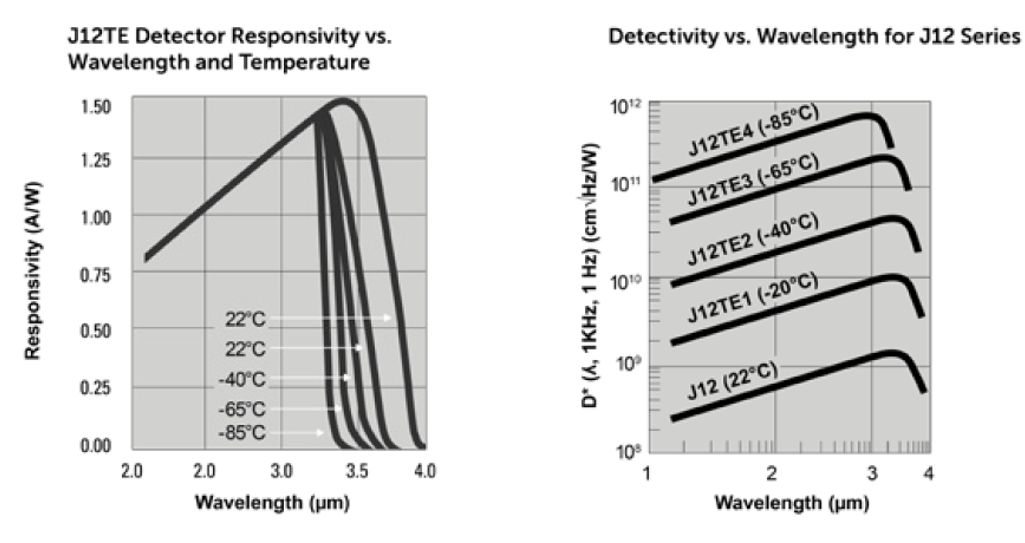
Figure 4: Responsivity and Detectivity vs wavelength for InAs sensors, highlighting different cutoff options at different temperatures.
Key Applications
InAs offers a strong balance of performance and complexity for mid-IR sensing without requiring full cryogenic cooling. Key applications include:
- Gas sensing: namely CO2 and hydrocarbons (CH2, C2H6 etc.), these gases have strong absorption features in the 3 – 4 µm region.
- Flame detection: InAs is well matched to the 3-3.5 µm emission band of hydrocarbon flames and hot CO2
- MWIR spectroscopy: such as elements for environmental and combustion diagnostics
- Broadband SWIR/MWIR radiometry: especially for process temperature measurement.
- Laser range-finding: at MWIR wavelengths for Er:YAG at 2.94 µm, HF/DF lasers
- Chemical sensing
Key Products
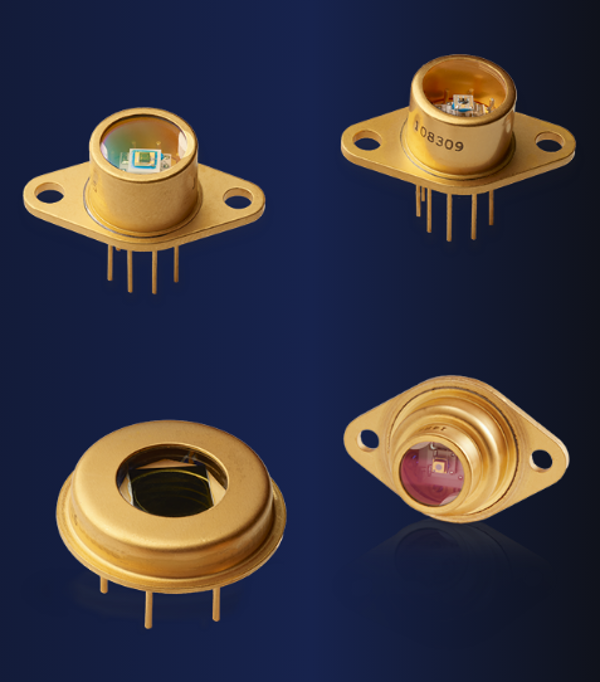
Teledyne Judson Technologies’ J12 series are TE-cooled InAs detectors with a 3.8 µm cut-off and photovoltaic operation, they deliver exceptional sensitivity for DC and low-frequency measurements, without the 1/f noise seen in photoconductive alternatives.
InSb (Indium Antimonide)
Key Features
- MWIR detection, typical spectral range 1.0-5.5 µm
- Peak response in 3.0-5.0 µm window
- Very high MWIR detectivity, among the highest of any available IR detector
- Low noise equivalent temperature difference (NETD), critical for thermal imaging
- Fast photoresponse
- Mature, large-format FPA technology is widely available
- Well known noise mechanisms enable predictable system-level performance modelling
- Some InSb devices are photovoltaic and can be operated at zero volts
Performance
Indium antimonide (InSb) is one of the earliest and most mature MWIR semiconductor detector materials. With a very narrow bandgap, InSb is sensitive to photons from below 2 µm out to approximately 5.5 µm, and is a near-perfect match to the atmospheric 3-5 µm MWIR transmission window, similar to InAs.
However, InSb operation almost universally requires liquid-nitrogen cooling to reach 77 K, where thermal noise is sufficiently suppressed to exploit the material's outstanding photon sensitivity. This results in increased system complexity and higher cost than TE-cooled or uncooled alternatives.
InSb has benefited from decades of development for demanding applications and has reached a high level of maturity as both single-element detectors and large-format FPAs. The resulting manufacturing base means high-quality InSb detectors are available with well-understood, reproducible performance characteristics.
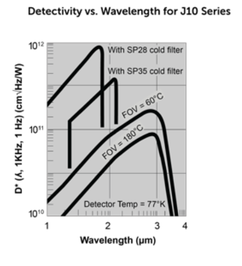
Figure 5: Detectivity vs wavelength for InSb sensors at 77 K temperatures, with different cold filters.
Key Applications
InSb is ideal for high-speed, high-sensitivity MWIR systems where cryogenic cooling is acceptable.
- Thermal imaging: Mostly for military/defense applications such as missile plume detection, IRST (Infrared Search and Track), targeting pods, and more
- High-speed MWIR imaging: combustion research, ballistic testing, aerodynamic heat signature studies
- Ground-based astronomy (M-band) and space-based remote sensing
- MWIR industrial thermography: process monitoring, predictive maintenance, non destructive testing for MWIR thermographic inspection (such as aerospace composites/welds)
- Medical and veterinary thermography
- MWIR spectroscopy in 3-5 um band
Key Products
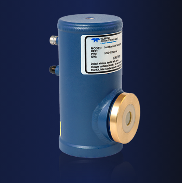
Teledyne Judson Technologies’ J10 series InSb sensors come with a M204 dewar as standard but can be packaged in a cryocooler with the same performance. Our J10 series are liquid nitrogen or cryocooled InSb detectors that operate from 1.0-5.5 µm.
MCT (Mercury Cadmiumn Telluride [HgCdTe])
Key Features
- Tunable SWIR/MWIR/LWIR detection, spectral range from 2.0-25 µm
- Bandgap is tunable vis Cd composition, MCT can match virtually any desired IR wavelength
- Photoconductor (PC) and photovoltaic (PV) MCT versions available: PC MCT ideal for LWIR/VLWIR sensing, PV MCT ideal for MWIR/LWIR sensing
- Very high detectivity and quantum efficiency across MWIR/LWIR
- Exceptional spectroscopy performance
- Fast response for both PC and PV variants
Performance
Mercury cadmium telluride (commonly written as MCT rather than HgCdTe) is the most versatile of all IR detector materials. It is a ternary alloy of mercury telluride (HgTe) and cadmium telluride (CdTe), with the defining property being that its bandgap is continuously tunable by adjusting the cadmium fraction.
MCT can therefore behave as a wide or very narrow bandgap semiconductor suitable for MWIR, LWIR or even VLWIR detection. This tunability is unique among commercial infrared materials and allows MCT to be engineered to match almost any specific wavelength requirement within the 2.0-25 µm range.
Teledyne Judson Technologies produces MCT in two distinct photodetector configurations: photoconductor (PC) and photovoltaic (PV), which differ fundamentally in their operating principle, circuit requirements, and optimal use cases.
Photoconductor (PC) MCT
In a photoconductor, incident photons generate free carriers that change the electrical conductivity of the semiconductor. An external bias is applied, and the detector's output is the change in current or voltage across a load resistor. PC MCT detectors are characterized by:
- High responsivity and sensitivity, especially at longer wavelengths and in VLWIR configurations
- Simpler device structure: PC devices are robust and can be produced in single-element and multi-element array formats
- Requirement for an applied bias voltage, which introduces Johnson noise and 1/f noise at low frequencies
- Excellent performance in the LWIR (8-12 µm) and VLWIR (12-25 µm) bands where photovoltaic operation becomes more difficult
- Broad wavelength coverage: a single material composition can cover several microns of spectral width, useful for broadband spectroscopy
PC MCT is therefore the detector of choice for demanding LWIR and VLWIR spectroscopy, including Fourier-transform infrared (FTIR) spectroscopy, atmospheric remote sensing, explosives and chemical agent detection (many threat signatures lie in the 8-12 µm fingerprint region), and astronomy.
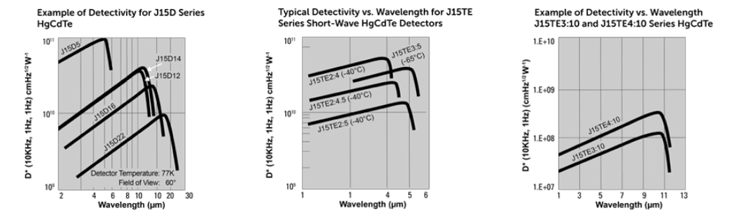
Figure 6: Detectivity vs wavelength for PC MCT sensors, with different cold filters.
Photovoltaic (PV) MCT
In a photovoltaic detector, a p-n junction is formed within the MCT material. Incident photons generate electron-hole pairs that are separated by the built-in electric field of the junction, producing a current without requiring an external bias. PV MCT detectors offer several important advantages over PC operation:
- Zero-bias (or very low bias) operation eliminates the dominant noise mechanism of the PC configuration, giving lower noise current and higher D*
- Better suited to high-frequency and high-speed applications, PV junctions can respond on nanosecond timescales
- More amenable to FPA integration: PV devices are read out by CMOS readout integrated circuits (ROICs) using bump-bonding, enabling large-format imaging arrays
- Lower power consumption: important for space and airborne platforms
PV MCT dominates in MWIR (3-5 µm) and standard LWIR (8-12 µm) high-performance detector and camera applications, including high-speed thermal imaging, laser detection, and remote sensing.
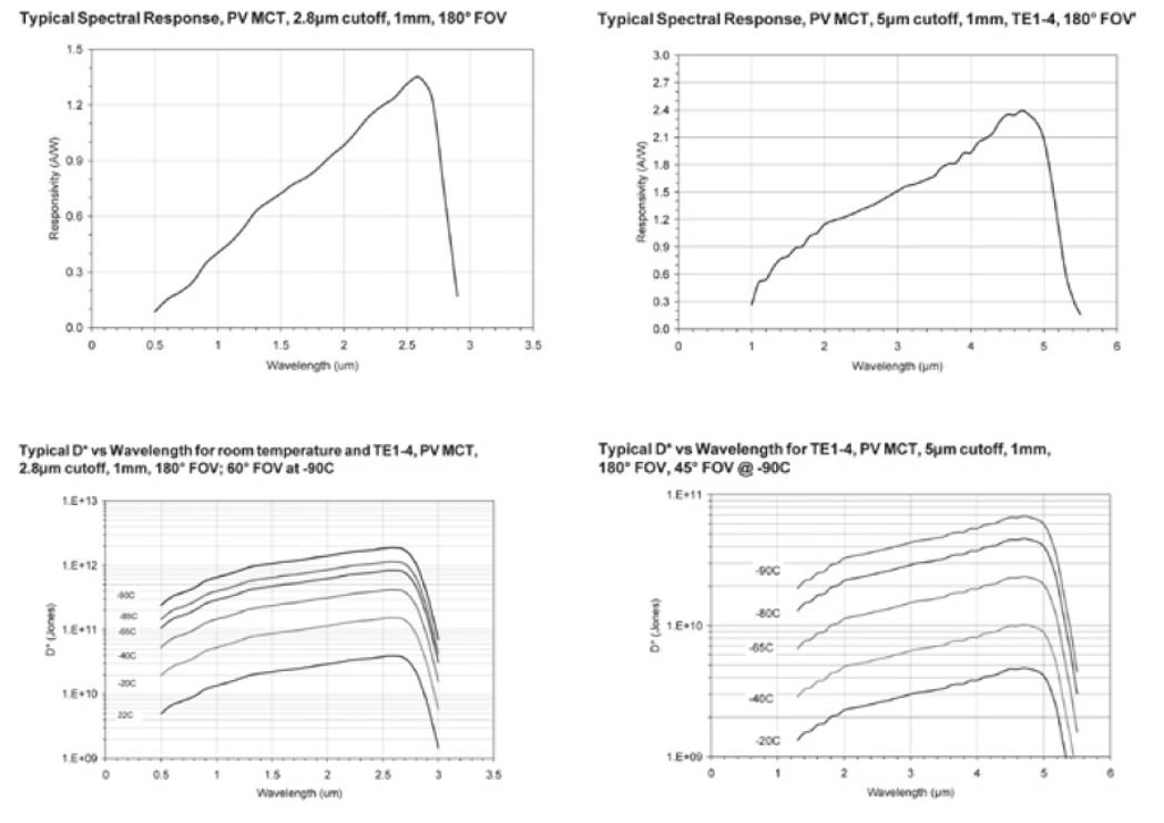
Figure 7: Detectivity vs wavelength for PV MCT sensors, with different cold filters.
Key Applications
MCT’s high level of tunability and performance across most of the IR spectrum allows for a wealth of use-cases and high-performance application options:
- FTIR and IR spectroscopy: broadband or tuned-composition MCT covers the complete molecular fingerprint region
- Hyperspectral imaging: benefits from access to a wide range of wavelengths
- MWIR/LWIR thermal imaging: high performance imaging for defense, surveillance, and targeting
- Laser power and pulse detection at CO (5.3 µm) and CO2 (10.6 µm) wavelengths
- Environmental monitoring: trace gas measurement, greenhouse gas sensing, climate research
- Chemical detection: MCT covers the 8-12 µm fingerprint absorption bands of most threat chemicals
- Medical diagnostics: exhaled breath analysis, non-invasive blood glucose sensing research
- Space instrumentation: requiring broad spectral coverage and radiation tolerance
Why Use MCT Over Microbolometers (VOx/Si)?
Another technology for IR detection is microbolometers, the dominant formats being vanadium oxide (VOx) and silicon (Si) variants. Back in the 1990s, microbolometers transformed the thermal imaging market as compact, low-cost LWIR camera options, and are often used in a wide range of applications.
However, for applications requiring sensitivity, speed and absolute performance, cooled MCT detectors occupy a different league entirely, being several orders of magnitude faster and more sensitive. Understanding the fundamental difference between these technologies is essential to making the right detector choise.
Microbolometers are thermal detectors, with IR radiation heating the resistive VOx/Si element and the resistance being read out as charge. With this method, detection is limited by the thermal time constant of the absorbing material, and by thermodynamic noise. In contact, MCTs are photon detectors, directly detecting IR photons that excite electrons across the semiconductor bandgap. This generates a fast, quantum and intrinsically sensitive method of detection. Below is a table summarizing the differences in these technologies.
| PC/PV MCT | VOx Microbolometer | |
| Detector Type | Photon detector | Thermal detector |
| Spectral Range | 2-25 µm (tunable) | 7-14 µm (LWIR) |
| Operating temperature | 77-200 K (cooled) | Room temperature |
| Sensitivity (D*) | Very high (10^10-10^11) | Moderate (~10^8-10^9) |
| Response Speed | Very fast (µs-ns) | Slow (ms) |
| NETD | <10 mK | ~30-50 mK typical |
| Uniformity | Excellent with calibration | Non-uniformity correction needed |
| SWaP (cooler) | Larger/heavier (requires cooler) | Compact, no cooler |
| Cost | Higher (cooler + detector) | Lower |
| Best Use Case | High-performance sensing, spectroscopy, fast laser, defense | Commercial thermography, security, drones |
For defense, scientific, medical, or industrial applications where sensitivity, speed, or spectral precision are non-negotiable, the additional cost and complexity of a cooled MCT system is justified and often the only technically viable option.
Key Products
PC MCT
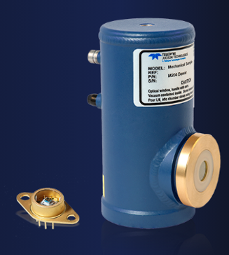
Teledyne Judson Technologies’ J15 series PC MCT sensors operate with a cut-off wavelength from 4-22.0 µm. These sensors feature a tunable bandgap, allowing users to optimize sensitivity based on the wavelengths of interest. They are available in both thermoelectrically cooled packages and cryocooled dewar-mounted sensors for liquid nitrogen cooling, ensuring ultimate performance.
We offer TE, liquid nitrogen, or cryocooling options across the J15 series.
PV MCT
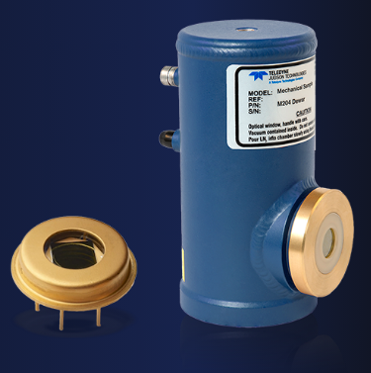
Teledyne Judson Technologies’ J19 series PC MCT sensors operate with a cut-off wavelength from 2.8-12.0 µm. MCT can be tailored to change the wavelength that the sensor is most sensitive to, allowing the user to optimize sensitivity to the wavelengths of interest and exclude unwanted longer-wavelength thermal radiation without needing expensive optical filters.
We offer TE or liquid nitrogen options across the J19 series.
T2SL (Type-II Superlattice)
Key Features
- MWIR/LWIR detection, typical spectral range 3.0-14 µm
- Tunable spectral range, like MCT
- Bandgap engineering can reduce dark current below MCT levels
- Improved uniformity
- Need for cooling is reduced/eliminated, while achieving performance similar to MCT/InSb
- All III-V material system, avoiding mercury allows easier production and integration
- Potential for dual/multi-band detection, such as simultaneous MWIR/LWIR
Performance
Type-II Superlattice (T2SL) detectors represent the most recent of the five material platforms covered in this article, emerging from fundamental research in the 1990s and maturing into a commercially significant technology over the past two decades.
T2SL structures are built from alternating ultra-thin nanometer layers of two III-V semiconductor materials, most commonly InAs and GaSb, or InAs and InAsSb. The quantum mechanical behavior of electrons and holes confined in these layers produces an engineered effective bandgap that does not exist in either bulk material alone. By adjusting the layer thicknesses and composition, the T2SL bandgap, and therefore the spectral cut-off, can be tuned across the MWIR and LWIR bands from ~3 µm to beyond 14 µm.
This tunability is similar in principle to that of MCT, but the T2SL platform offers several material and manufacturing advantages that are attracting considerable interest, particularly from the defense, space, and high-performance imaging communities.
Ongoing materials research continues to close the performance gap with MCT, and in some configurations T2SL already matches or exceeds MCT performance at equivalent temperatures. However, T2SL is less mature than MCT, while the technology is advancing rapidly T2SL can’t match MCT and InSb in terms of large-format FPA uniformity, 1/f noise, and surface passivation.
Key Applications
T2SL represents a next-generation engineered material platform with strong potential advantages in stability and manufacturability:
- Space remote sensing: radiation hardness and absence of mercury are advantages for space qualification
- High-performance MWIR/LWIR imaging: Next-generation defense platforms for missile seeking, target discrimination, hyperspectral imaging and more
- Scientific/research instrumentation: where engineered spectral response and HOT operation are valuable.
- Thermography/gas sensing: emerging commercial applications where a higher operating temperature reduces system cost
Key Products
Teledyne Judson Technologies’ J24 series T2SL detectors are available in both room temperature and TE-cooled configurations, operating with a cut-off wavelength tailored to specific infrared applications. have lower Auger recombination rates compared to other materials like MCT, which can lead to lower dark currents and potentially higher operating temperatures.
We offer uncooled or TE cooled options across the J24 series.
Why Choose Teledyne Judson Technologies?
Teledyne Judson Technologies differentiates not only through material offerings but through implementation quality.
Broadest Material Portfolio
Few suppliers offer: InGaAs, InAs, InSb, MCT, and T2SL from a single source. This allows system designers to compare materials directly, optimize based on application rather than supplier limitation, and scale from NIR to LWIR within one vendor ecosystem
Customization Capability
Teledyne Judson Technologies provides:
- Custom spectral cutoff tuning (MCT composition control)
- Custom detector geometries
- Integrated preamplifiers
- TE or cryogenic packaging
- Application-specific assemblies
This is critical for OEM instrumentation builders.
High Detectivity & Low Noise Optimization
Key performance advantages include:
- Low dark current engineering
- Precision material growth control
- High uniformity
- Application-matched cooling solutions
- Integrated detector + preamp solutions to reduce system noise
System-Level Expertise
Teledyne Judson detectors are engineered for integration into:
- FTIR systems
- Gas analyzers
- Process control instrumentation
- Scientific spectrometers
- Aerospace systems
Support includes:
- Application engineering
- Thermal design guidance
- Noise optimization
- Integration assistance
| Application | Recommended Material |
| NIR spectroscopy (1-1.7 µm) | InGaAs |
| Extended SWIR (2-2.6 µm) | Extended InGaAs |
| 2-4 µm gas sensing | InAs or MCT |
| High-speed MWIR imaging | InSb |
| High-performance FTIR | MCT |
| LWIR spectroscopy | MCT |
| Emerging MWIR/LWIR systems | T2SL |
Selecting the correct infrared detector material is not simply a wavelength decision, it is a tradeoff between sensitivity, cooling complexity, speed, cost, and long-term system stability.
Teledyne Judson Technologies provides one of the most comprehensive IR material portfolios in the industry, enabling engineers to select the optimal detector architecture, not just the available one.