Lensless EUV Metrology
Dr. Sven Weerdenburg
Experimental Computational Imaging with EUV & Soft X-Ray, ASML
Background
Dr. Sven Weerdenburg recently graduated from the Optics Research group of the Imaging Physics department of the TU Delft and is now working on EUV imaging at ASML. His thesis focus was on EUV metrology of semiconductor-like structures. Common metrology techniques, such as electron microscopy, provide high spatial resolution but lack the penetration depth required to retrieve 3D information when inspecting increasingly complex semiconductor structures. Additionally, when applied to EUV lithography mask metrology, they do not directly yield relevant contrast or sensitivity, as defects observed under an electron beam can appear drastically different from those seen with EUV light.
EUV imaging provides high spatial resolution and UV sensitivity but, “A big problem with EUV imaging is that you don't have conventional optics available in this wavelength range (10 to 30 nm) and EUV optics (mirrors) with a sufficient or high enough numerical aperture are incredibly expensive.” mentions Dr. Weerdenburg.
Here, we present a published research project [Shao et al. 2024] where Dr. Weerdenburg investigated the possibility of 'lensless imaging', namely the concept of using ptychography for next generation EUV metrology. “We illuminate a semiconductor-like target, and we capture the diffraction patterns with a full-vacuum EUV CCD camera.” says Dr. Weerdenburg, discussing the experimental setup shown in Fig.1. The EUV beam scans the sample surface and collects diffraction patterns, from which amplitude and phase information are extracted to computationally retrieve the high-resolution spatial image of the sample. This analysis method allows user to detect defects on semiconductors or lithography masks, especially those in the EUV range.
The improved control in the EUV range leverages the methodology presented here as a potentially helpful quality assurance method, especially for a semiconductor production pipeline.
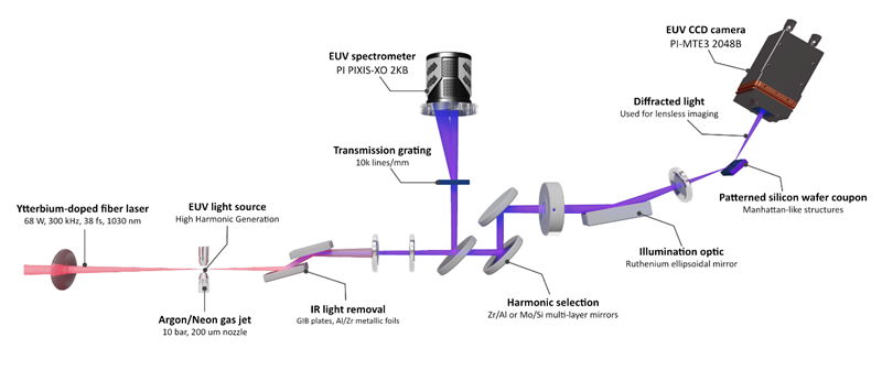
Figure 1: Schematic of the main optical elements in the experimental setup. This setup is also featured in the following YouTube video: LINX EUV lensless imaging setup - Delft University of Technology.
Challenge
There are a range of factors that make this novel experimental method a challenge. Firstly, the final spatial resolution of a reconstructed image strongly depends on the imaging setup geometry, and the quality of the diffraction patterns acquired with the sensor. In addition, as EUV light does not propogate through air, EUV processes such as lithography during semiconductor production must be under vacuum conditions.
Another requirement from the detector is high sensitivity in the EUV range, combined with chip cooling capabilities to enable minimal noise for optimal signal acquisition. Dr. Weerdenburg also mentions: “The camera becomes the only optical part in the lensless optical system in that sense, and the size of the camera then primarily defines your numerical aperture of your imaging system, so that the larger the camera detector, the larger the NA.”
To optimize the signal detection, a sensor with a large physical size, high EUV sensitivity, low noise, and full compatibility in-vacuum is required.
One of the things I really like about the [PI-MTE3] camera is the LightField software that came with it. It's a robust package, easy to control and you have a lot of freedom in terms of things you can tune within the main package.”
Dr. Sven Weerdenburg
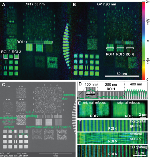
Figure 2: A+B) Ptychographic reconstructions of nanostructures on the wafer sample at wavelength 17.30 nm (A) and 17.93 nm (B). The brightness and hue of the image represent the amplitude and phase of the complex-valued object, respectively. The reconstructed objects show shifted field-of-views as the probes at different wavelengths illuminate different areas on the sample. C) SEM image of the wafer sample with various types of structures and manufacturing defects for comparison. D) Profile of the chirped grating in ROI 1 consisting of 200 nm, 100 nm, and 50 nm lines with varying spacing. Inset: the finest part of the chirped grating with 150 nm pitch and 50 nm linewidth. E) Gratings in squared areas ROI 2 (with a manufacturing defect) and ROI 3, before (left) and after (right) refocusing for enhancing contrast. F) Zoom-in of the reconstructed structures in ROI 4–6. Due to the non-uniform sample resolution in the reflection geometry, only the horizontal grating and the horizontal part of the 2D grating can be resolved. Taken from [Shao et al. 2024].
Solution
The PI-MTE3 CCD camera is a great match for the experimental requirements of this project, offering vacuum compatibility, a direct-detection window ranging from UV to soft X-ray, and a high quantum efficiency peak in the EUV range (10-124 eV). The PI-MTE3 sensor can be deep cooled to -50°C and enables highly sensitive signal collection with minimal noise. The large physical size of the sensor is optimal for this project, providing a large numerical aperture in the ptychography setting and thereby improved image quality. The four-port readout architecture offers a 7 to 10 times higher frame rate and can be useful for fast diagnostics.
All the features of the PI-MTE3 and the full range of Teledyne Princeton Instruments solutions are steered within Lightfield, a user-friendly software package flexible enough to be optimized for different experiments.
Reference
Shao, Y., Weerdenburg, S., Seifert, J., Urbach, H. P., Mosk, A. P., & Coene, W. (2024). Wavelength-multiplexed multi-mode EUV reflection ptychography based on automatic differentiation. Light: Science & Applications, 13, Article 196. https://doi.org/10.1038/s41377-024-01558-3